


Waveguides
Definition: spatially inhomogeneous transparent structures for guiding light
More specific terms: planar waveguides, channel waveguides, optical fibers
German: Wellenleiter
Category: fiber optics and waveguides
How to cite the article; suggest additional literature
Author: Dr. Rüdiger Paschotta
An optical waveguide is a spatially inhomogeneous structure for guiding light, i.e. for restricting the spatial region in which light can propagate. Usually, a waveguide contains a region of increased refractive index, compared with the surrounding medium (called cladding). However, guidance is also possible, e.g., by the use of reflections, e.g. at metallic interfaces. Some waveguides also involve plasmonic effects at metals.
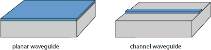
Most waveguides exhibit two-dimensional guidance, thus restricting the extension of guided light in two dimensions and permitting propagation essentially only in one dimension. An example is the channel waveguide shown in Figure 1. The most important type of two-dimensional waveguide is the optical fiber. There are also one-dimensional waveguides, often called planar waveguides.
Waveguide Fabrication
There are many different techniques for fabricating dielectric waveguides. Some examples are:
- Planar waveguides can be fabricated on various crystal and glass materials with epitaxy or with polishing methods. The waveguide may be made on the top of the device (as shown on the left side of Figure 1), but it can also be placed between other solid layers.
- Channel waveguides on semiconductor, crystal and glass materials can be made with lithographic methods in combination with, e.g., epitaxy, ion exchange, or thermal indiffusion. It is possible to make a buried waveguide by growing an additional layer on top of the waveguide. That may lead to lower propagation losses and a more symmetric mode profile.
- Optical fibers can be fabricated by drawing from a preform, which is a large glass rod with a built-in refractive index profile. Fibers can again be drawn into waveguides of further reduced dimensions, in the extreme case resulting in nanofibers.
- Waveguides can be written into transparent media (e.g. glasses or crystals) with focused and pulsed laser beams, exploiting laser-induced breakdown and related phenomena. In glasses, the affected volume often exhibits a somewhat increased refractive index, which can be directly used for guiding light. In crystals, the refractive index may be decreased; one then has to treat some region around the desired waveguide region.
The trade-offs between different fabrication techniques can be complicated. They can involve aspects such as cost, flexibility and reproducibility of manufacturing, propagation losses, possible side effects on the material (e.g. via heating or indiffused materials), optimum mode size and symmetry for coupling to other waveguides, etc.
Waveguide Modes
For waveguides with large extensions, ray optics are often used for describing the propagation of injected light. Such a description, however, becomes invalid when interference effects occur, and this is particularly the case for very small waveguide dimensions. In that case, a wave description of the light is required – normally on the basis of Maxwell's equations, often simplified with approximating assumptions.
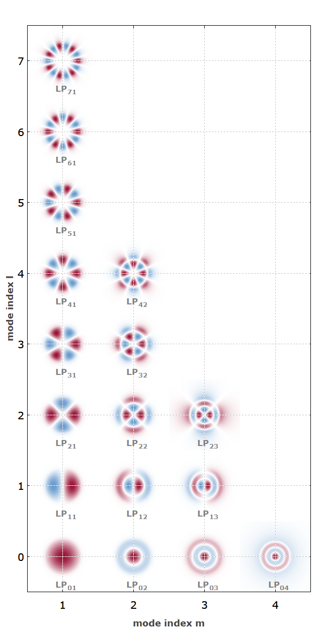
It is common to consider the field distribution for a given optical frequency and polarization in a plane perpendicular to the propagation direction. Of special interest are those distributions which do not change during propagation, apart from a common phase change. Such field distributions are associated with so-called waveguide modes. As an example, Figure 2 shows the guided modes of a multimode fiber. Each mode has a so-called propagation constant, the imaginary part of which quantifies the phase delay per unit propagation distance. A fiber also has a large number of unguided modes (cladding modes), which are not restricted to the vicinity of the fiber core.
Any initial field distribution, which may be generated at the beginning of the waveguide, can be decomposed into a linear combination of the field distributions of the guided waveguide modes, plus some function which can not be expressed as such a combination. The latter part corresponds to light which can not be guided. Depending on the type of waveguide, the not guided light may propagate in the cladding or may be reflected. The propagation of the guided part is easily calculated, using a linear combination of the waveguide modes with local expansion coefficients calculated from the propagation constants of the modes.
A waveguide with a small transverse spatial extension and/or a small refractive index difference (small numerical aperture) may be able to guide only a single transverse mode (for a given optical frequency and polarization) and no higher-order modes; it is then called a single-mode waveguide (→ single-mode fibers). The field distribution after a certain propagation distance then always resembles the constant mode field distribution, independent of the initial field distribution, provided that the unguided modes have been lost (e.g. in the cladding). Multimode waveguides are those supporting several or even many guided modes (sometimes many thousands).
Some types of waveguides (e.g. the channel waveguide on the right side of Figure 1) exhibit modes with strongly asymmetric intensity profiles. It also happens that guided modes exist only for one polarization direction, or that the modes for different polarization directions have very different properties.
Various properties such as the propagation loss, the bend sensitivity (for fibers), the propagation constant and the chromatic dispersion (see below) can substantially depend on the type of guided mode.
Waveguide Dispersion
Confinement of light in a waveguide leads to wave vectors which are tilted against the propagation direction. This affects the phase delay per unit length and thus the chromatic dispersion properties (→ waveguide dispersion). For example, the dispersion of a photonic crystal fiber with small mode area can be anomalous in the visible spectral region, although the silica material would have normal dispersion.
Plasmonic Waveguides for Nano Optics
For various applications, for example in the context of photonic integrated circuits, it is of great interest to strongly localize light in waveguides to dimensions far below the optical wavelength. Here, dielectric waveguides exhibit serious limitations. For example, although nanofibers can have diameters far below the wavelength, the electric field distributions of light guided in nanometer-scale fibers extend far beyond dielectric structure. Therefore, new waveguide technologies based on other physical guiding mechanisms are investigated. A promising field is that of nanoplasmonics [11], where nanometer-scale metallic structures embedded in dielectric materials are used. In that way, it is possible to obtain much more localized field distributions than possible with dielectric structures alone. However, the propagation losses are typically very high. Additional challenges are to efficiently couple light into such structures and to realize various passive and active photonic components such as strong bends, couplers, filters, amplifiers and detectors.
Applications
The applications of waveguides are manifold. Some examples are:
- Optical fibers allow the transmission of light over long distances, e.g. for optical fiber communications.
- On photonic integrated circuits, as used e.g. in silicon photonics, waveguides guide light between different optical components.
- In the future, silicon waveguides on digital processor chips and polymer waveguides in circuit boards may be used for fast optical data transmission between components of computers.
- Some waveguides are used for maintaining high optical intensities over appreciable lengths, e.g. in nonlinear devices such as frequency doublers and Raman lasers. Active (amplifying) waveguides are used in waveguide lasers and amplifiers. Important examples are fiber lasers and fiber amplifiers.
- A waveguide can be used for stripping off higher-order transverse modes, thus acting as a mode cleaner.
- In some cases, an interaction of the guided light with material in the evanescent field is used, e.g. in certain waveguide sensors.
- Waveguides can also be employed for splitting and combining light beams, e.g. in integrated optical interferometers.
Suppliers
The RP Photonics Buyer's Guide contains 13 suppliers for waveguides. Among them:
Questions and Comments from Users
Here you can submit questions and comments. As far as they get accepted by the author, they will appear above this paragraph together with the author’s answer. The author will decide on acceptance based on certain criteria. Essentially, the issue must be of sufficiently broad interest.
Please do not enter personal data here; we would otherwise delete it soon. (See also our privacy declaration.) If you wish to receive personal feedback or consultancy from the author, please contact him e.g. via e-mail.
By submitting the information, you give your consent to the potential publication of your inputs on our website according to our rules. (If you later retract your consent, we will delete those inputs.) As your inputs are first reviewed by the author, they may be published with some delay.
Bibliography
| [1] | R. A. Soref and J. P. Lorenzo, “Single-crystal silicon: a new material for 1.3 and 1.6 μm integrated-optical components”, Electron. Lett. 21 (21), 953 (1985), doi:10.1049/el:19850673 |
| [2] | R. V. Ramaswamy and R. Srivastava, “Ion-exchanged glass waveguides: a review”, IEEE J. Lightwave Technol. 6 (6), 984 (1988), doi:10.1109/50.4090 |
| [3] | B. Schüppert et al., “Optical channel waveguides in silicon diffused from GeSi allow”, Electron. Lett. 25 (22), 1500 (1989), doi:10.1049/el:19891007 |
| [4] | N. Takato et al., “Silica-based single-mode waveguides on silicon and their application to guided-wave optical interferometers”, IEEE J. Lightwave Technol. 6 (6), 1003 (1988), doi:10.1109/50.4091 |
| [5] | K. M. Davis et al., “Writing waveguides in glass with a femtosecond laser”, Opt. Lett. 21 (21), 1729 (1996), doi:10.1364/OL.21.001729 |
| [6] | M.-K. Chin et al., “High-index-contrast waveguides and devices”, Appl. Opt. 44 (15), 3077 (2005), doi:10.1364/AO.44.003077 |
| [7] | H. Hu et al., “Lithium niobate ridge waveguides fabricated by wet etching”, IEEE Photon. Technol. Lett. 19 (6), 417 (2007), doi:10.1049/el:19950195 |
| [8] | J. I. Mackenzie, “Dielectric solid-state planar waveguide lasers: a review”, J. Sel. Top. Quantum Electron. 13 (3), 26 (2007), doi:10.1109/JSTQE.2007.897184 |
| [9] | M. E. Solmaz et al., “Compact bends for achieving higher integration densities for LiNbO3 waveguides”, IEEE Photon. Technol. Lett. 21 (9), 557 (2009), doi:10.1109/LPT.2009.2014569 |
| [10] | J. Hu and C. R. Menyuk, “Understanding leaky modes: slab waveguide revisited”, Adv. Opt. Photon. 1, 58 (2009), doi:10.1364/AOP.1.000058 |
| [11] | D. K. Gramotnev and S. I. Bozhevolnyi, “Plasmonics beyond the diffraction limit”, Nature Photon. 4, 83 (2010), doi:10.1038/nphoton.2009.282 |
| [12] | D. Geskus et al., “Giant optical gain in a rare-earth-ion-doped microstructure”, Adv. Mater. 24 (10), OP19 (2012), doi:10.1002/adma.201101781 |
| [13] | A. W. Snyder and J. D. Love, Optical Waveguide Theory, Chapman and Hall, London (1983) |
| [14] | Website on "Optical waveguides: numerical modeling" |
See also: channel waveguides, fibers, nanofibers, numerical aperture, modes, mode coupling, higher-order modes, effective mode area, mode field converters, integrated optics, waveguide lasers, frequency doubling, waveguide dispersion, silicon photonics
and other articles in the category fiber optics and waveguides
 |
If you like this page, please share the link with your friends and colleagues, e.g. via social media:
These sharing buttons are implemented in a privacy-friendly way!