Dielectric Coatings
Definition: thin-film coatings made of transparent dielectric materials, e.g. for laser mirrors or anti-reflection coatings
Alternative terms: thin-film coatings, interference coatings, multilayer coatings
More general term: optical coatings
More specific terms: anti-reflection coatings, absorbing coatings, black coatings, mirror coatings
German: dielektrische Beschichtungen
How to cite the article; suggest additional literature
Author: Dr. Rüdiger Paschotta
Dielectric coatings, also called thin-film coatings or interference coatings, consist of thin (typically sub-micron) layers of transparent dielectric materials, which are deposited on a substrate. Their function is essentially to modify the reflective properties of the surface by exploiting the interference of reflections from multiple optical interfaces. They can be used for highly reflecting laser mirrors or partially transmissive output couplers, for dichroic mirrors (treating different wavelengths differently), for anti-reflection coatings, for various kinds of optical filters (e.g. for attenuation of certain wavelength regions), beam splitters, heat reflectors, solar cell covers, and thin-film polarizers. While simple single-layer coatings are often used as anti-reflection coatings, dielectric mirrors normally use dozens of thin-film layers, sometimes even more than 100. A typical mirror design is the simple Bragg mirror, but there are many more sophisticated mirror designs.
The typical kind of dielectric coating consists of discrete layers with substantially different refractive indices. However, there are also gradient-index coatings for rugate filters, where the refractive index is varied continuously. That can be achieved, for example, by gradually varying the chemical composition of the material during growth.
In many cases, the coating substrate is some kind of glass, with a wide transparency range and high optical quality (low bubble content), a very smooth surface (after proper polishing), and high durability. However, dielectric coatings can also be applied to crystalline materials, e.g., as anti-reflection coatings on nonlinear crystals for nonlinear frequency conversion and Pockels cells, or on semiconductor devices such as edge-emitting laser diodes, vertical cavity surface-emitting lasers, and photodiodes. A further area of increasing importance is the fabrication of dielectric coatings on polymers (plastic materials), as plastic optics are increasingly used due to their competitive properties, e.g. in terms of price and the ease of fabricating non-spherical surfaces (e.g. for aspheric lenses).
The material properties of the dielectric films can substantially depend on the used fabrication method (see below) and fabrication parameters such as the substrate temperature or partial pressures of various substances. Compared with the ordinary bulk materials of nominally the same chemical composition, thin-film layers often have a reduced packing density and a reduced refractive index. When designing a dielectric coating for fabrication on a certain coating machine, one should have the refractive index data for that machine under the used conditions, as the differences can be substantial.
Dielectric coatings are often applied to optical glasses, but they can also be used for plastic optics.
Designing Multilayer Coatings
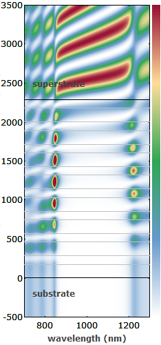
The reflection properties of dielectric multilayer coatings can be adapted to many different applications by using suitable coating designs. A coating design involves the choice of dielectric materials (typically, two different ones) and of all the layer thickness values. The article on dielectric mirrors contains some details on design methods.
Fabrication and Choice of Materials
This section applies mostly to coatings for glasses and crystalline materials, even though some aspects also apply to polymer optics. The fabrication of dielectric mirrors is usually based on one of the following techniques:
- Electron beam deposition involves the evaporation of material in a crucible by heating with an electron beam, which is generated from a hot filament and focused with a magnetic field. In the vacuum chamber, the evaporated material moves to the substrate, which can be covered with a mechanical shutter as soon as the right amount of material has been deposited. The target substrate is heated to improve the quality. For typical coating materials, the obtained thin films tend to be somewhat porous, leading to a reduced density and subsequently to a reduced refractive index. The optical properties can then exhibit a significantly increased temperature dependence, as water may fill the pores, and may be driven out of the coating at elevated temperatures. This can be a problem for some sensitive steep-edge filter designs, for example.
- A similar method uses evaporation by resistive heating of the crucible.
- Ion-assisted deposition (IAD) essentially works like e-beam evaporation, but involves an additional ion beam (consisting of oxygen and/or argon ions) which hits the target substrate. The comparatively high energy of the ions allows a reordering of the deposited material, leading to denser coatings, even without heating the substrate. The method works well for oxide coatings (e.g. SiO2 or TiO2), which can have a similar quality as those obtained with IBS (see below). IAD is not suitable, however, for fluoride materials, which tend to disassociate.
- Ion beam sputtering (IBS) uses an ion beam which, after neutralization with a second filament, hits a metal or metal oxide target to sputter material to the substrate. The flux and energy of the ions can be controlled independently and precisely. IBS generates fairly uniform, non-porous coatings with good adhesion and very low surface roughness (possibly below 1 Å), and is well reproducible. However, it is relatively slow, requires expensive equipment and materials, and is less flexible than other methods.
- Advanced plasma reactive sputtering (APRS) involves the sputtering of thin metal films, which are subsequently oxidized in a separate oxygen plasma region of the chamber. Separate magnetron sources are used for the different coating materials. APRS combines a high precision and high density of the coatings (similar to that of IBS) with a high speed (comparable to that of evaporation techniques).
In any case, one starts with some homogeneous substrate material such as BK7 glass, fused silica, or CaF2, which is often pre-processed with method for preparing a very clean surface. Common coating materials are oxides such as SiO2, TiO2, Al2O3 and Ta2O5, and fluorides such as MgF2, LaF3 and AlF3. The layers obtained are usually amorphous, with a density which can (depending on the fabrication technique) deviate from that of bulk material by more than 10%. Electron-beam deposition typically generates materials with lower densities, and thus also a lower refractive index. Such porous coatings have microvoids which can fill up with water when exposed to humid air; in effect, the refractive index and thus the whole properties of the coating depend on the humidity. Ion-assisted deposition and particularly ion beam sputtering achieve a higher density and accordingly a lower dependence on humidity. The optical damage threshold can also depend on the fabrication method.
Materials with a high refractive index contrast need to be used for high reflectivity mirrors, and particularly when a large reflection bandwidth is required. However, the chosen materials should also allow for fabrication with high optical quality and should have high stability under given environmental conditions (concerning laser wavelength and intensity, operation temperature, humidity, etc.).
Important aspects for the selection of a fabrication technique are
- the suitability for given coating materials
- the precision of the layer thickness values (which may be increased with automatic control involving in-situ growth monitoring)
- the optical quality of the deposited layers (influencing e.g. the scattering losses)
- the ability of the coatings to withstand high optical intensities
- the uniformity of layer thickness values over a larger area
- the consistency (reproducibility) and stability of obtained refractive indices
- the required substrate temperature
- the time required for the growth
For example, ion-assisted deposition produces TiO2 films which are more compact and thus more stable and homogeneous and have a higher refractive index, compared with e-beam evaporation, which however is a faster process. The reason is essentially that TiO2 has a tendency to grow in low-density nanostructures, which can be destroyed (compacted) by irradiation with high-energy ions.
In-situ growth monitoring is crucial for obtaining precisely controlled layer thickness values. One uses the fact that the optical reflection or transmission properties can be used during the process to monitor the thickness of the currently grown layer, so that the growth process for a layer can be stopped at exactly the right time. A challenge is that the growth temperature usually differs considerably from the intended operating temperature of the coating, and accurate temperature-dependent refractive index data are often not available.
Apart from the basic fabrication method, the process parameters such as the substrate temperature and growth rate can also be important for the quality. The details are often confidential proprietary information of the fabricators.
The requirements on the substrate material vary, depending on the application. For highly reflective mirrors, important technical aspects can be the surface roughness, but also the thermal expansion coefficient (which is ideally similar to that of the coating materials) and the thermal conductivity. (In high-power lasers, residual absorption in the coating can cause some bulging of the mirror surface, inducing thermal lensing.) For mirrors with partial transmission of the light (e.g. for output couplers of lasers, or dichroic mirrors), it is also important to have good transparency of the substrate in the relevant wavelength range in addition to high optical quality. The back side may have to be given an anti-reflection coating.
For anti-reflection coatings on laser crystals and particularly on nonlinear crystals with anisotropic thermal expansion, but also for substrates with small curvature radii or for optical devices exposed to some chemicals, it can be a challenge to obtain coatings which are sufficiently stable. Optical damage, often occurring at microscopic defects, can also be a problem for devices operating with high optical intensities.
Bragg mirrors can also be made of crystalline semiconductor materials, grown e.g. with molecular beam epitaxy (MBE) or with metal-organic chemical vapor deposition (MOCVD) (→ crystalline mirrors). Such mirrors are often parts of some larger structures, such as vertical cavity surface-emitting lasers.
The article on dielectric mirrors explains in some detail how the optical properties of dielectric coatings can be calculated, and which aspects are important for designing such structures.
Suppliers
The RP Photonics Buyer's Guide contains 136 suppliers for dielectric coatings. Among them:

Intrinsic Crystal Technology
Intrinsic Crystal Technology offers dielectric coatings for the ultraviolet, visible, near infrared, mid infrared and far infrared spectral ranges.

EKSMA OPTICS
We offer dielectric laser mirrors for fixed, narrowband or broadband wavelength applications covering UV, VIS and IR. Wide selection of round, elliptical or custom shapes as well as plano, spherical, cylindrical surface mirrors and substrates are available.

VisiMax Technologies
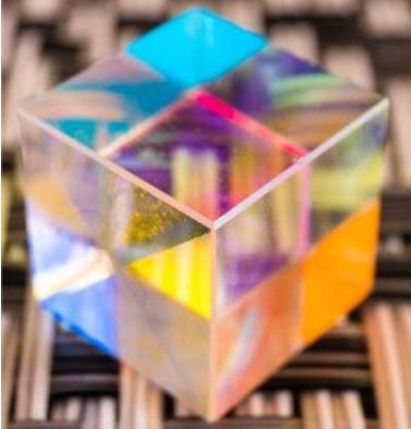
VisiMax offers a wide range of optical coating products, including anti-reflection coatings, optical filters and mirror and beam splitter coatings. They can be applied to most optical materials including glass, plastics, molded polymer optics, and semiconductor materials. We also produce protective vacuum-applied or dip-applied coatings for adding extra durability to your optical components.


Laseroptik
LASEROPTIK can fabricate dielectric coatings with a range of methods including electron beam evaporation (EBE), ion assisted desposition (IAD), ion plating (IP), magnetron sputtering (MS) and ion beam sputtering (IBS). With our high precision machinery, we can produce accurate coatings for a wide range of wavelengths, substrate materials and applications. In addition to a large selection of from-stock optics, we offer coatings with refined custom designs.
Knight Optical
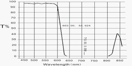
We offer a range of dielectric coatings for optimum reflectivity. Available for a variety of components including beamsplitters, front-surface mirrors and rod and cone mirrors, to name but a few, our dielectric options include visible, near-infrared (NIR), infrared (IR) (2000 nm +) and large parts (1000 mm).

Shanghai Optics
Shanghai Optics can provide all types of anti-reflective, high reflective, and partial reflective coatings. We produce a wide variety of coatings from a single layer of anti-reflective coating to complex multi-layer dielectric stacks. Types of dielectric coatings are BBAR, V-coatings, dual wavelength coatings, and sharp cut-on and cut-off filters.
Questions and Comments from Users
Here you can submit questions and comments. As far as they get accepted by the author, they will appear above this paragraph together with the author’s answer. The author will decide on acceptance based on certain criteria. Essentially, the issue must be of sufficiently broad interest.
Please do not enter personal data here; we would otherwise delete it soon. (See also our privacy declaration.) If you wish to receive personal feedback or consultancy from the author, please contact him e.g. via e-mail.
By submitting the information, you give your consent to the potential publication of your inputs on our website according to our rules. (If you later retract your consent, we will delete those inputs.) As your inputs are first reviewed by the author, they may be published with some delay.
Bibliography
| [1] | J. R. McNeil et al., “Ion-assisted deposition of optical thin films: low energy vs. high energy bombardment”, Appl. Opt. 23 (4), 552 (1984), doi:10.1364/AO.23.000552 |
| [2] | H. Sankur and R. L. Hall, “Thin-film deposition by laser-assisted evaporation”, Appl. Opt. 24 (20), 3343 (1985), doi:10.1364/AO.24.003343 |
| [3] | P. J. Martin, “Ion-based methods for optical thin film deposition”, J. Mat. Science 21 (1), 1 (1986), doi:10.1007/BF01144693 |
| [4] | H. A. MacLeod, Thin-Film Optical Filters, Adam Hilger Ltd., Bristol (1986) |
| [5] | A. Thelen, Design of Optical Interference Coatings, McGraw–Hill (1989) |
| [6] | N. Kaiser (ed.), Optical Interference Coatings, Springer, Berlin (2003) |
See also: dielectric mirrors, dichroic mirrors, anti-reflection coatings, rugate filters, beam splitters, thin-film polarizers, crystalline mirrors, The Photonics Spotlight 2007-03-09
and other articles in the category photonic devices
 |




If you like this page, please share the link with your friends and colleagues, e.g. via social media:
These sharing buttons are implemented in a privacy-friendly way!